India aims to become a semiconductor manufacturing hub. What are the challenges faced by the semiconductor industry in India? Mention the salient features of the India Semiconductor Mission.
India aims to become a semiconductor manufacturing hub. What are the challenges faced by the semiconductor industry in India? Mention the salient features of the India Semiconductor Mission.
India's semiconductor market, valued at $38 billion in 2023, is projected to reach $100-110 billion by 2030. The India Semiconductor Mission (ISM) represents India's strategic push towards technological sovereignty.
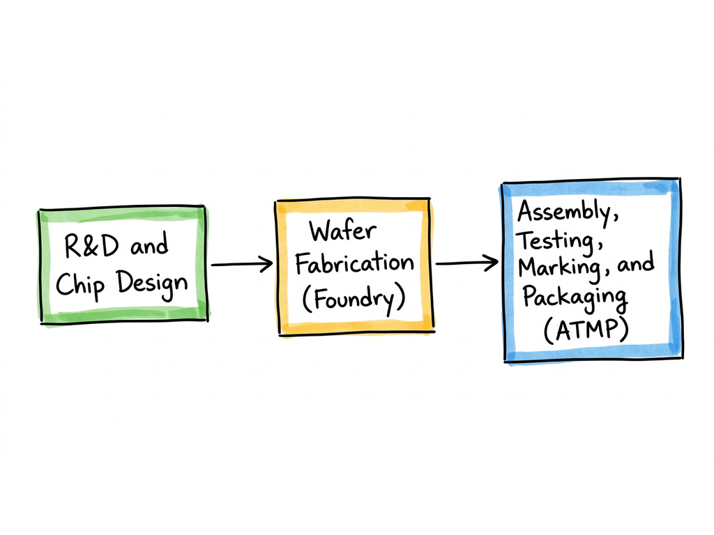
Semiconductor manufacturing process from design to packaging
Challenges Faced by the Semiconductor Industry in India
Infrastructure and Power Constraints
- Unreliable Power Supply: Continuous 24/7 fab operations require quality power (99.9999% uptime), currently a challenge in India.
- Inadequate Clean Room Facilities: Global fabs like TSMC use Class 1 cleanrooms, India has limited facilities.
- Poor Logistics Network: High-value semiconductor imports often pass through congested ports; no specialised “chip corridor” yet.
- Water Scarcity: A single fab can consume ~10 million litres/day (example: Intel’s fabs in Arizona), posing stress in water-deficit states.
- Limited Testing Infrastructure: Shortage of advanced testing and validation facilities and India depends on Taiwanese/US labs for high-end chip testing.
Resource and Skill Challenges
- Critical Material Shortage: Reliance on imports of rare earths (mainly from China, ~85% market share).
- Skilled Workforce Gap: Report by Electronics Sector Skills Council: shortage of 250,000–350,000 chip engineers by 2027.
- High Capital Investment: Setting up an advanced fab costs $15–20 billion, compared to $5 billion for a steel plant.
- Technology Access: Restrictions on advanced semiconductor manufacturing technologies. US export bans on sub-7 nm technologies limit India’s entry into cutting-edge segments.
- Long Gestation Period: 5–7 years before returns, deterring private investors compared to IT services or startups.
Salient Features of the India Semiconductor Mission
| Component | Allocation | Purpose | Value Addition |
|---|---|---|---|
| Manufacturing Incentives | ₹62,900 crore | Semiconductor fab setup | ~50% cost subsidy, in line with US CHIPS Act and EU Chips Act |
| Infrastructure Development | ₹10,000 crore | Modernizing Mohali Lab | Potential hub for compound semiconductors & R&D |
| Design Linked Incentive | ₹1,000 crore | Design capabilities | India has ~30 fabless startups (e.g., Saankhya Labs) |
Key Strategic Elements
- Employment Generation: Target 1 million direct/indirect jobs by 2026, aiding demographic dividend.
- Global Partnerships: MoUs with TSMC (Taiwan), Samsung (Korea), Micron (USA), and Japan for knowledge transfer.
- State-level Support: Dholera (Gujarat): Micron’s $2.7 bn plant; Karnataka: design & R&D cluster.
- Research Focus: IIT Madras, IISc Bengaluru working on indigenous fab tech & compound semiconductors (GaN, SiC).
- Supply Chain Integration: Focus on local sourcing of wafers, chemicals, testing units under Atmanirbhar Bharat.
India’s semiconductor journey faces structural bottlenecks in infrastructure, resources, and skills. Yet, through ISM, global tie-ups, and design-led innovation, India can position itself as a trusted alternative to China and a key player in the $574 billion global semiconductor market.
Answer Length
Model answers may exceed the word limit for better clarity and depth. Use them as a guide, but always frame your final answer within the exam’s prescribed limit.
In just 60 sec
Evaluate your handwritten answer
- Get detailed feedback
- Model Answer after evaluation
Model Answers by Subject
Crack UPSC with your
Personal AI Mentor
An AI-powered ecosystem to learn, practice, and evaluate with discipline