Semicon 2.0: India Semiconductor Mission 2.0 Outlay, Pillars and Targets
ISM 2.0 notified with a ₹1.27 lakh crore outlay across six pillars - design, equipment, fabs, packaging, R&D and talent. Targets: 200 design startups, 1 lakh technicians, 400 universities.
Sep, 2026
•10 min read
Overview
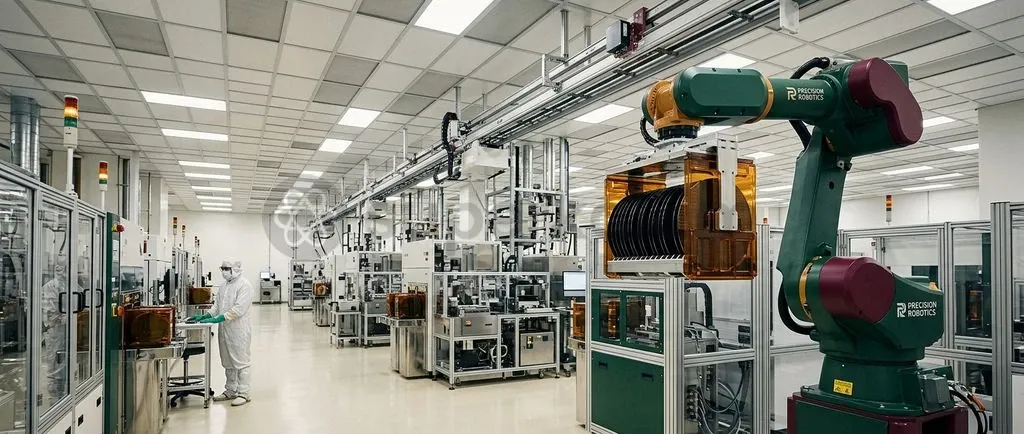
Semicon 2.0 marks India's policy transition from chasing multi-billion-dollar trophy silicon foundries toward building full-stack domestic supply chain depth. The policy incentivises upstream specialty chemicals, equipment manufacturing, and domestic intellectual property retention.
Approved by the Union Cabinet with an enhanced outlay of ₹1,27,500 crore, the updated framework addresses structural gaps exposed during the initial phase of the India Semiconductor Mission. Rather than competing solely for bleeding-edge sub-5nm fabrication plants, the policy anchors fiscal subsidies across six strategic pillars. This strategy balances immediate industrial demand in automotive and power electronics with long-term technological sovereignty and geopolitical resilience.
Why in the News: The Genesis and Vision of Semicon 2.0
The Union Cabinet approved the Semicon 2.0 programme on 15 July 2026 to accelerate the domestic semiconductor ecosystem across six comprehensive pillars. As of September 2026, the India Semiconductor Mission (ISM) operates under an expanded mandate to bridge raw material vulnerabilities, advanced packaging gaps, and intellectual property shortfalls.
India's domestic semiconductor market is expanding rapidly from approximately $38 billion in 2023 toward an estimated $100 to $110 billion by 2030. Surging demand across automotive electronics, industrial automation, 5G telecommunications, and consumer devices has elevated microelectronics into a pillar of national economic security.
The original Semicon India programme achieved notable ground-level momentum, approving 12 semiconductor manufacturing projects representing a cumulative investment exceeding ₹1.64 lakh crore across six states. However, heavy reliance on imported silicon ingots, photoresists, electronic-grade specialty gases, and foreign design architectures demonstrated that front-end assembly alone cannot guarantee strategic self-reliance.
Discuss with Superkalam
What is the total financial outlay approved by the Union Cabinet for the Semicon 2.0 programme?
Ask NowWhat Was ISM 1.0 and What Were Its Core Limitations?
The initial India Semiconductor Mission, launched under the Ministry of Electronics and Information Technology (MeitY), focused heavily on attracting leading-edge silicon fabrication plants through direct capital expenditure support. While this strategy established intent, real-world execution faced structural constraints in capital access, technology transfer partnerships, and ecosystem readiness.
The initial framework confronted several distinct operational and strategic bottlenecks:
- Disproportionate Focus on Leading-Edge Fabs: Early efforts prioritised advanced logic nodes below 28 nanometres (nm), where global players faced prohibitive capital costs and intellectual property transfer barriers.
- Capital Dispersal and High Entry Barriers: Constructing commercial front-end fabs demands $5 billion to $10 billion per facility, creating extreme fiscal sensitivity during global market downcycles.
- Neglect of Upstream Inputs: The original framework did not provide dedicated fiscal support for electronic-grade chemicals, precision gases, cleanroom equipment, and specialised substrates.
- Design Incentive Underutilisation: The design ecosystem faced commercialisation barriers, with domestic startups struggling to translate approved architectures into tape-outs and high-volume purchase orders.
Recognising these commercial dynamics, Indian policymakers shifted focus toward Outsourced Semiconductor Assembly and Test (OSAT) units, Assembly, Testing, Marking, and Packaging (ATMP) plants, and mature nodes of 28nm and above. Mature nodes require significantly lower capital outlays of $300 million to $3 billion and offer faster operational turnaround times of 18 to 24 months.
ISM 1.0 vs Semicon 2.0: Comparing Strategic Priorities and Fiscal Architecture
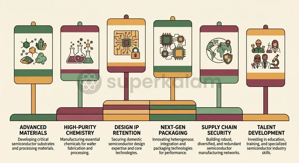
Semicon 2.0 restructures national industrial policy by shifting from isolated fab subsidies to an integrated, vertically linked semiconductor supply chain. The revised architecture redistributes capital incentives across raw materials, equipment manufacturing, packaging, and design intellectual property.
| Dimension | ISM 1.0 (Initial Framework) | Semicon 2.0 (Current Architecture) |
|---|---|---|
| Primary Policy Focus | Standalone front-end wafer fabrication facilities and legacy ATMP | Full-stack integration covering upstream materials, advanced packaging, and domestic IP |
| Total Fiscal Outlay | Initial ₹76,000 crore incentive package | Enhanced ₹1,27,500 crore total outlay across six pillars |
| Upstream Inputs & Equipment | No dedicated subsidy framework for chemicals, gases, or equipment | Dedicated fiscal incentives under Pillar 2 for manufacturing tools, gases, and materials |
| Packaging Architecture | Basic wire-bond assembly and legacy testing facilities | 35% fiscal subsidy for 2.5D/3D packaging and heterogeneous integration |
| DLI Ownership Mandate | Generic commercialization targets without strict equity controls | Mandatory minimum 51% domestic equity to prevent IP flight |
| Strategic Anchor Facility | Ambiguous commercial concession roadmap for public infrastructure | ₹4,500 crore modernization of Semi-Conductor Laboratory (SCL) Mohali |
Under Pillar 4 of Semicon 2.0, the government offers a 35% fiscal subsidy on a pari-passu basis for capital expenditure in advanced packaging. This incentive covers 2.5D and 3D multi-die packaging, heterogeneous integration, and wafer-level packaging, subject to a minimum capital investment threshold of ₹1,000 crore.
Discuss with Superkalam
Why are electronic-grade specialty chemicals and ultra-pure gases considered the real operational 'moat' in semiconductor manufacturing?
Ask NowBeyond Silicon Fabs: Why Equipment, Chemicals, and Gases Form the Real Moat
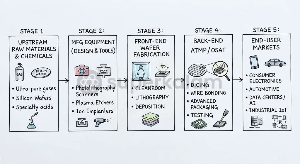
Semiconductor supply chain sovereignty depends far more on specialised chemicals, ultra-pure gases, and precision fabrication tools than on concrete cleanroom shells. Modern chip fabrication involves hundreds of sequential processing steps, each demanding raw materials refined to extreme purity standards.
Pillar 2 of Semicon 2.0 introduces dedicated incentives for domestic manufacturing and research in upstream inputs. These inputs form the operational moat of global chip manufacturing:
- Ultra-Pure Electronic Gases: High-volume fabrication relies on continuous supplies of nitrogen, silane, phosphine, and high-purity argon. Minor contamination at parts-per-billion levels degrades entire silicon batches.
- Specialty Photolithography Chemicals: Advanced etching and patterning require electronic-grade photoresists, specialised polymers, developers, and ultra-pure hydrofluoric acid.
- Silicon Wafers and Substrates: Raw polysilicon must be transformed into single-crystal ingots and sliced into defect-free wafers before front-end fabrication begins.
- Precision Manufacturing Equipment: Wafer steppers, chemical vapour deposition chambers, and plasma etchers represent high-margin, concentrated technologies currently controlled by a handful of global firms.
Encouraging domestic joint ventures in chemical synthesis and precision engineering insulates Indian foundries from external export controls and shipping bottlenecks.
Revamping Design-Linked Incentives (DLI): Overcoming IP and Domestic Scaling Bottlenecks
The Design-Linked Incentive (DLI) scheme underwent major policy restructuring under Semicon 2.0 to resolve chronic intellectual property retention bottlenecks. While India accounts for a substantial share of the global chip design workforce, domestic engineers historically worked as design service contractors for multinational corporations rather than developing homegrown, patent-protected architectures.
The initial phase of the DLI scheme delivered modest commercial conversion, approving 24 chip design projects out of more than 60 applicant enterprises. Early startup beneficiaries faced severe funding constraints when attempting to scale from software simulation to physical prototype fabrication, lacking commercial access to overseas foundry slots.
To prevent domestic intellectual property flight, the revised DLI guidelines mandate that eligible design consortia must maintain at least 51% domestic equity ownership. This equity ceiling permits up to 49% foreign strategic participation while guaranteeing that core architectural patents, royalties, and commercial licensing rights remain anchored in India.
The Ministry of Electronics and IT has simultaneously expanded foundational infrastructure, deploying advanced Electronic Design Automation (EDA) tools through the C-DAC ChipIN Centre to over 320 academic institutions. This institutional framework has trained more than 68,000 engineering students under the Chips to Startup (C2S) initiative, creating a pipeline of skilled circuit designers.
Discuss with Superkalam
How can the 51% domestic equity rule under the DLI scheme be applied to prevent IP flight while attracting foreign venture capital?
Ask NowGeopolitics of the Global Chip Race: iCET, Quad Partnerships, and Supply Chain Resilience
Global microelectronics production exhibits extreme geographic vulnerability, driving major industrial nations toward aggressive bilateral and multilateral de-risking strategies. Concentrated manufacturing clusters in East Asia remain vulnerable to geopolitical friction, seismic disruptions, and regional supply chain blockades.
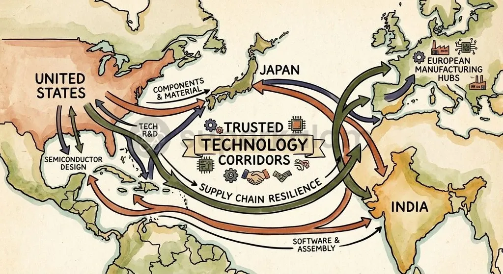
Global foundry capacity remains heavily asymmetric, with Taiwan producing over 60% of total worldwide foundry output and approximately 90% of advanced sub-7nm logic chips. This geographic concentration has prompted the United States, Japan, the European Union, and India to construct trusted semiconductor corridors.
| Alliance / Framework | Strategic Focus Area | Key Operational Objectives |
|---|---|---|
| TRUST Framework (US-India iCET upgrade) | Hardware security & supply chain integrity | Establishing secure hardware architectures and cross-border supply chain verification |
| Quad Semiconductor Initiative | Supply chain mapping & critical minerals | Stress-testing supply networks, tracking strategic materials, and securing rare earths |
| Bilateral Technology Corridors | Packaging & advanced tool R&D | Advanced packaging partnerships with Japan; research and tool linkages with the EU |
India and the United States transitioned their critical technology cooperation from the Initiative on Critical and Emerging Technologies (iCET) into the upgraded TRUST framework. This institutional platform secures semiconductor supply lines, coordinates joint research in compound semiconductors, and establishes transparent packaging standards across partner nations.
Structural Headwinds: Ultra-Pure Water, Power Quality, and the Specialist Talent Deficit
Operating commercial semiconductor foundries requires uncompromising utility infrastructure and complex environmental mitigation systems that test municipal capacities. A failure in basic resource stability can compromise months of high-precision manufacturing.
The physical requirements of commercial chip manufacturing introduce formidable engineering hurdles:
- Extreme Water Consumption: A commercial wafer fabrication plant consumes 2 to 5 million gallons of ultra-pure water (UPW) per day, treated to parts-per-trillion purity standards to eliminate microscopic contaminants during photolithography.
- Hazardous Wastewater and Effluent Treatment: Fabrication processes generate toxic waste streams containing hydrofluoric acid, heavy metal residues, and persistent per- and polyfluoroalkyl substances (PFAS), requiring on-site Zero Liquid Discharge (ZLD) neutralization systems.
- Millisecond Power Reliability: Front-end fabs demand continuous, millisecond-resilient electrical power supported by dedicated high-voltage substation redundancy. A voltage sag lasting a few milliseconds can ruin an entire production line during multi-week fabrication cycles.
- Specialised Talent Shortage: While India excels in digital chip architecture and software simulation, it faces a structural deficit of experienced cleanroom technicians, yield-enhancement engineers, and process metallurgists.
State industrial development agencies must establish dedicated industrial corridors equipped with dual-grid power feeds, tertiary wastewater recycling plants, and integrated hazardous waste treatment facilities.
Discuss with Superkalam
Compare the strategic advantages and capital risks of pursuing mature nodes (28nm+) versus leading-edge nodes (sub-5nm) for India's domestic industrial base.
Ask NowWay Forward: Building Lasting Technological Sovereignty Beyond Subsidies
Achieving genuine technological resilience in semiconductors requires moving beyond fiscal subsidies toward enduring institutional capability, strategic public infrastructure, and deep industrial research. Capital subsidies attract initial factory construction, but sustained domestic competitiveness depends on indigenous innovation.
Policy execution should focus on four structural priorities:
- Transforming Public R&D Infrastructure: The Central Government has allocated ₹4,500 crore to modernize the Semi-Conductor Laboratory (SCL) in Mohali, upgrading its 180nm fabrication line into an open-access national R&D tape-out center without privatising the facility.
- Expanding Compound Semiconductor Ecosystems: Prioritise niche compound semiconductors such as Gallium Nitride (GaN) and Silicon Carbide (SiC), which are vital for electric vehicle powertrains, high-voltage railway traction, and defence radar systems.
- Integrating into Global Tier-1 Supply Chains: Encourage domestic component makers to supply high-precision quartz components, ceramic end-effectors, and specialty valves to leading global fabrication tool manufacturers.
- Institutionalising Industry-Academia Linkages: Align national engineering curricula directly with foundry requirements through structured cleanroom apprenticeships and fab-attachment fellowships.
Key Takeaways
- Policy Transformation: Semicon 2.0 expands India's semiconductor strategy with an enhanced outlay of ₹1,27,500 crore, shifting priorities from isolated front-end foundries to full-stack supply chain depth across materials, equipment, and advanced packaging.
- Strategic Pragmatism: The mission targets mature nodes (28nm and above) and advanced packaging (35% capex subsidy), addressing immediate domestic market demand in automotive and industrial electronics.
- Intellectual Property Protection: Revised DLI rules enforce a minimum 51% domestic equity ownership threshold to ensure homegrown design architectures and patent rights remain in India.
- Resource and Infrastructure Intensity: Commercial fabrication demands 2 to 5 million gallons of ultra-pure water daily, millisecond-stable electrical power grids, and Zero Liquid Discharge chemical neutralization facilities.
- Public R&D Anchor: The modernisation of SCL Mohali with ₹4,500 crore provides domestic startups and researchers with a dedicated prototyping and tape-out foundry.
Mains Question
"Semiconductor supply chain sovereignty depends far more on specialised chemicals, ultra-pure gases, and precision fabrication tools than on concrete cleanroom shells." In the light of this statement, critically analyse the strategic reorientation from ISM 1.0 to the Semicon 2.0 framework. (15 Marks)
Evaluate NowMains Question
Despite possessing a significant share of the global chip design workforce, domestic intellectual property retention has remained a chronic bottleneck for India. Elucidate how the revamped Design-Linked Incentive (DLI) scheme and foundational training initiatives address this challenge. (10 Marks)
Evaluate NowPractice MCQs
QUESTION 1
With reference to India's semiconductor policy framework under Semicon 2.0, consider the following statements:
- It enhances the total fiscal outlay from ₹76,000 crore under the initial framework to ₹1,27,500 crore distributed across six pillars.
- Pillar 4 offers a 35% fiscal subsidy on a pari-passu basis for advanced packaging, subject to a minimum capital investment threshold of ₹1,000 crore.
- Under the revised Design-Linked Incentive (DLI) guidelines, eligible design consortia must maintain at least 51% domestic equity ownership.
Which of the statements given above are correct?
QUESTION 2
Consider the following statements regarding the strategic shift from ISM 1.0 to Semicon 2.0:
- ISM 1.0 faced challenges due to a heavy policy emphasis on bleeding-edge logic nodes below 28nm, where capital barriers and IP transfer restrictions were high.
- Mature nodes of 28nm and above require significantly lower capital outlays and offer shorter operational turnaround times compared to sub-28nm fabs.
- Semicon 2.0 excludes public-sector semiconductor facilities from modernization to prioritize purely private design consortia.
Which of the statements given above is/are correct?
QUESTION 3
With reference to the foundational inputs and upstream elements of semiconductor manufacturing described in the article, consider the following statements:
- Pillar 2 of Semicon 2.0 introduces dedicated fiscal incentives for manufacturing tools, specialty chemicals, and electronic-grade gases.
- Minor contamination in ultra-pure gases like silane and phosphine at parts-per-billion levels does not affect silicon yield in commercial fabrication.
- The Chips to Startup (C2S) initiative and C-DAC ChipIN Centre have deployed EDA tools across over 320 academic institutions.
Which of the statements given above is/are correct?
QUESTION 4
Which of the following strategic reasons best explains the mandate requiring a minimum 51% domestic equity ownership under the revamped Design-Linked Incentive (DLI) scheme?
QUESTION 5
Consider the following statements regarding the global semiconductor landscape and international initiatives:
- Taiwan accounts for over 60% of total worldwide foundry output and approximately 90% of advanced sub-7nm logic chips.
- The TRUST Framework forms part of the US-India iCET upgrade aimed at hardware security and supply chain integrity.
Which of the statements given above is/are correct?