Semicon 2.0 Framework: India's Full-Stack Semiconductor Strategy
India shifts from basic packaging to full-stack chip sovereignty under an expanded ₹1,27,500 crore push across fabrication, raw materials, and strategic IP.
Sep, 2026
•9 min read
Overview
The Union Cabinet approved the Semicon 2.0 framework with an outlay of ₹1,27,500 crore. The plan shifts India from basic downstream packaging toward a full-stack semiconductor ecosystem covering raw materials, fabrication, and intellectual property.
The revised policy provides targeted fiscal incentives for 300-mm wafer fabrication, domestic chip design, and upstream supply chain inputs like specialty chemicals and equipment. As of August 2026, the framework establishes long-term policy support to protect supply chains and advance technological sovereignty across strategic and commercial sectors.
Why is Semicon 2.0 in the News?
The Ministry of Electronics and Information Technology (MeitY) notified the operational guidelines for all six strategic pillars under Semicon 2.0 on August 31, 2026. This rollout establishes the regulatory and financial architecture to disburse the approved outlay of ₹1,27,500 crore across domestic industry.
Global supply realignments have accelerated the push for domestic semiconductor supply chain resilience. India's initial push under the India Semiconductor Mission drew strong investor interest. However, it also exposed major gaps in upstream inputs, local intellectual property generation, and specialised tooling. The updated framework directly targets these gaps to anchor high-value manufacturing domestically.
Background: Evolution from the India Semiconductor Mission (ISM 1.0)
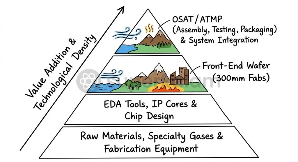
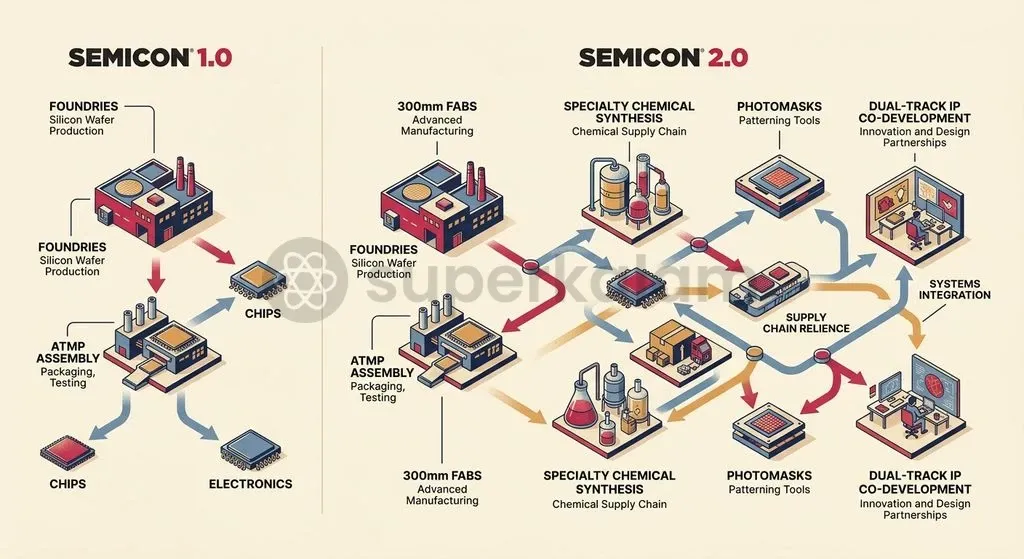
The India Semiconductor Mission originated under the Modified Programme for Semiconductors and Display Fab Ecosystem to build domestic manufacturing capabilities. The initial phase focused heavily on attracting silicon foundries and establishing Assembly, Testing, Marking, and Packaging (ATMP) alongside Outsourced Semiconductor Assembly and Test (OSAT) units.
While packaging facilities took off, domestic manufacturing units still relied on imported silicon wafers, photoresists, specialty gases, and foreign IP. Packaging alone leaves domestic industry exposed to sudden supply shocks and export controls.
The transition to Semicon 2.0 marks an evolution in industrial strategy. It moves India from isolated manufacturing facilities toward a self-sustaining full-stack domestic ecosystem.
Discuss with Superkalam
Recall the capex subsidy percentage provided for upstream chemical and equipment infrastructure under the Semicon 2.0 framework.
Ask NowWhat is Semicon 2.0: Core Objectives and Expanded Scope
Semicon 2.0 expands government support across every stage of the semiconductor value chain, targeting foundational inputs rather than final assembly alone. The core goal is building indigenous technological capability while cutting dependence on single-source geographic corridors.
Under the framework notified by MeitY, the policy establishes specific fiscal benchmarks across distinct segments of the value chain:
- Silicon Wafer Fabrication: The framework offers calibrated fiscal support of 40% of project capital expenditure for establishing large 300-mm silicon wafer fabrication units with a minimum threshold investment of ₹20,000 crore.
- Upstream Ecosystem Support: The policy provides 30% capital expenditure support for the domestic production of semiconductor manufacturing equipment, specialty chemicals, industrial gases, photoresists, and photomasks.
- Modernisation of Strategic Infrastructure: The Union Government approved a dedicated ₹4,500 crore modernisation plan for the state-owned Semiconductor Laboratory (SCL) in Mohali to scale its fabrication capacity by 100 times for student prototypes and strategic applications.
- Long-Term Technology Roadmap: The mission formalises a long-term technology trajectory aiming to master advanced manufacturing capabilities at 3-nanometre and 2-nanometre nodes by 2035.
Key Strategic Pillars: Moving from Assembly to Full-Stack Ecosystem
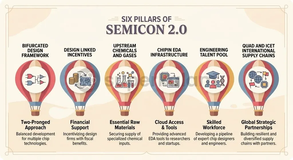
The Ministry of Electronics and Information Technology structured Semicon 2.0 around six operational pillars designed to systematically tackle bottlenecks across the entire value chain.
1. Bifurcated Chip Design Framework
Pillar 1 splits chip design into two operational tracks to balance national security requirements with market-driven innovation:
- Strategic Track: The Centre for Development of Advanced Computing (C-DAC) co-owns critical intellectual property alongside developing fabless teams for sensitive defence, space, and telecommunications deployments.
- Commercial Track: Early-stage fabless startups receive financial assistance through seed funding up to ₹15 crore or 50% of project cost to stimulate commercial enterprise.
2. Design Linked Incentive (DLI) Scheme
The Design Linked Incentive scheme provides direct financial backing for product commercialisation. Its deployment-linked component offers a 9% reimbursement on net sales turnover over five years, capped at ₹30 crore per application and ₹120 crore per company, to speed up market adoption of indigenous integrated circuits.
3. Upstream Chemical and Equipment Infrastructure
Semicon 2.0 incentivises the domestic synthesis of electronic-grade specialty chemicals and precision tooling. By offering 30% capex subsidies to chemical refiners, gas purifiers, and mask makers, the policy shields domestic fabs from overseas logistical bottlenecks.
4. Advanced Academic Tooling and Infrastructure
Access to expensive chip design software is democratised through the ChipIN Centre at C-DAC Bangalore. The facility has provided industry-grade Electronic Design Automation (EDA) tools to over 332 academic institutions and 105 startups, clocking over 2 crore tool-usage hours.
5. Specialised Human Capital Development
Human capital forms the core talent engine of the mission. The initial Chips to Start-up (C2S) programme trained 85,000 semiconductor engineers across Indian universities. Building on this, the government set an expanded target to train an additional 1,00,000 specialised engineers under Semicon 2.0.
6. Global Supply Chain Integration
The framework coordinates domestic incentives with bilateral and plurilateral partnerships to secure supply continuity. Strategic collaboration is formalised through the Quad Semiconductor Supply Chain Initiative and the US-India Initiative on Critical and Emerging Technology (iCET).
Discuss with Superkalam
Explain why relying solely on downstream packaging (ATMP/OSAT) leaves a domestic semiconductor industry vulnerable to global supply shocks.
Ask NowComparing Semicon 1.0 vs Semicon 2.0: Structural Shifts
The structural shift between the initial policy iteration and Semicon 2.0 reflects a transition from opportunistic packaging assembly to systematic industrial planning.
| Dimension | India Semiconductor Mission (ISM 1.0) | Semicon 2.0 Framework |
|---|---|---|
| Primary Focus Area | Foundries and downstream ATMP and OSAT assembly units | Full-stack ecosystem including equipment, chemicals, and design |
| Total Fiscal Outlay | ₹76,000 crore initial budgetary commitment | ₹1,27,500 crore expanded allocation |
| Wafer Fab Incentives | Flat uniform capital expenditure support | 40% project capex support for 300-mm fabs with ₹20,000 crore threshold |
| Upstream Inputs | No dedicated capex support for raw material supply | 30% capex support for gases, chemicals, photomasks, and tools |
| Design IP Strategy | Broad financial assistance for fabless entities | Bifurcated Strategic and Commercial tracks with C-DAC IP co-ownership |
| Talent Target | 85,000 trained personnel via the C2S scheme | Additional 1,00,000 engineers targeted under expanded curricula |
Why Semiconductor Manufacturing Matters for India's Economic Security
Semiconductor components form the core building blocks of modern industrial competitiveness, critical infrastructure, and national defence. Domestic fabrication safeguards against geopolitical supply weaponisation and international transit bottlenecks.
From a balance-of-payments standpoint, local fabrication reduces the rising import bill from automotive electronics, consumer hardware, and industrial automation. Creating an integrated ecosystem also drives domestic patent creation, keeping high-value design revenue within the country.
Industry projections underline the scale of this opportunity. According to estimates by the India Electronics and Semiconductor Association (IESA), the Semicon 2.0 policy environment has the potential to catalyse over ₹5,00,00 crore in cumulative private investments across the semiconductor value chain over the next five to seven years.
Discuss with Superkalam
How can an early-stage Indian fabless startup utilize both the Commercial Design Track and the Design Linked Incentive (DLI) scheme to bring a new chip to market?
Ask NowKey Hurdles: Capital Costs, Supply Chain Dependencies, and Talent Gaps
Semiconductor manufacturing faces severe structural and resource constraints that require sustained, multi-decade policy coordination.
- Utility Infrastructure Requirements: Commercial fabrication facilities demand 2 to 10 million gallons of ultra-pure water daily alongside uninterrupted, harmonic-free power grids, presenting major utility challenges for state host governments.
- Prohibitive Capital Intensity: Advanced node manufacturing requires multi-billion-dollar recurring capital investments, where machinery suffers rapid obsolescence within three to five operational years.
- Raw Material Import Vulnerability: Upstream chemical purification and silicon crystal growth remain concentrated in select economies, meaning domestic fabs remain exposed to global supply shocks until local supply chains mature.
- Specialised Experience Deficits: While India holds a substantial portion of global chip design talent, the domestic workforce lacks hands-on industrial fabrication experience in operating cleanroom environments.
Global Policy Lessons: Synthesising US and Taiwan Precedents
International industrial frameworks offer vital structural lessons for India's execution of the Semicon 2.0 policy.
- United States (Capital Subsidies with Geopolitical Guardrails): The United States enacted the CHIPS and Science Act of 2022, deploying $52.7 billion in direct manufacturing subsidies alongside 25% advanced manufacturing investment tax credits to onshore fabrication facilities. However, the American framework introduced strict export-control guardrails and national security conditionalities that limited operational flexibility for recipient firms. India's fiscal policy avoids restrictive conditionalities, but must match the sustained, predictable funding mechanisms provided by Western tax credit structures.
- Taiwan (Institutional R&D and Cluster Density): Taiwan built global market dominance by combining institutional state-backed research with geographic industrial concentration. The Industrial Technology Research Institute (ITRI) served as a foundational R&D incubator that spun off commercial champions like TSMC, while the Hsinchu Science Park co-located foundries, testing labs, chemical suppliers, and equipment technicians in a dense geographic cluster.
- Strategic Application for India: India's strategy of revitalising SCL Mohali with a ₹4,500 crore allocation mirrors Taiwan's early public research incubation model. However, whereas Taiwan avoided single-vendor dependency through organic cluster density, India must ensure its distributed academic network via the ChipIN Centre translates directly into commercially viable manufacturing clusters rather than isolated design hubs.
Discuss with Superkalam
Analyse the strategic trade-offs of the government co-owning intellectual property through C-DAC versus allowing complete private IP ownership in sensitive sectors.
Ask NowWay Forward: Building a Resilient and Self-Sustaining Chip Industry
Building a competitive semiconductor ecosystem requires shifting from short-term financial grants to long-term institutional and infrastructural enablement.
- Guarantee Dedicated Utility Corridors: State governments must provide statutory guarantees for ultra-pure water recycling and redundant electrical substations adjacent to designated semiconductor manufacturing zones.
- Encourage Domestic Commercial Procurement: Public procurement norms should mandate the preferential purchase of indigenously designed and fabricated chips in public transport, energy meters, and government communications networks.
- Expand SCL Mohali as an Open Foundry: Modernising SCL Mohali into a common-access R&D foundry will allow domestic startups and universities to fabricate low-volume pilot runs without relying on foreign silicon foundries.
- Deepen Global Plurilateral Alignments: Diplomatic channels under the Quad and iCET frameworks should be leveraged to secure critical mineral supplies and technology transfer agreements for advanced packaging nodes.
Key Takeaways
- The Union Cabinet approved the Semicon 2.0 framework with a total financial outlay of ₹1,27,500 crore to construct a full-stack domestic semiconductor ecosystem.
- Fiscal support includes 40% project capex for 300-mm wafer fabrication plants and 30% capex support for upstream equipment, industrial gases, and specialty chemicals.
- The chip design policy is bifurcated into a Strategic Track co-owned with C-DAC for defence hardware and a Commercial Track offering seed support up to ₹15 crore.
- The ChipIN Centre at C-DAC Bangalore has extended advanced EDA tools to 332 institutions and 105 startups, logging over 2 crore usage hours to support domestic engineering capabilities.
- The state-owned Semiconductor Laboratory (SCL) in Mohali will receive ₹4,500 crore to scale wafer fabrication capacity by 100 times for prototyping and strategic applications.
- Structural execution challenges remain centred on massive continuous capital expenditure, ultra-pure water supplies (2-10 million gallons daily), stable power grids, and fabricating at advanced 3nm/2nm technology nodes by 2035.
Mains Question
"The transition from basic downstream packaging under ISM 1.0 to a full-stack ecosystem under Semicon 2.0 marks a structural shift in India's industrial strategy." Elucidate. (10 Marks)
Evaluate NowMains Question
In light of vulnerabilities exposed by global supply chain disruptions, evaluate the role of the six strategic pillars under the Semicon 2.0 framework in advancing India's technological sovereignty and economic security. (15 Marks)
Evaluate NowPractice MCQs
QUESTION 1
With reference to the fiscal incentives notified under the Semicon 2.0 framework, consider the following statements:
- It provides 40% project capital expenditure support for establishing 300-mm silicon wafer fabrication units with a minimum threshold investment of ₹20,000 crore.
- It offers 30% capital expenditure support for the domestic production of upstream inputs, including specialty chemicals, photomasks, and manufacturing equipment.
- It mandates the complete disinvestment and privatization of the state-owned Semiconductor Laboratory (SCL) in Mohali.
Which of the statements given above is/are correct?
QUESTION 2
Consider the following statements regarding the Bifurcated Chip Design Framework and the Design Linked Incentive (DLI) Scheme under Semicon 2.0:
- Under the Strategic Track, the Centre for Development of Advanced Computing (C-DAC) co-owns critical intellectual property with developing teams for sensitive defence and space applications.
- The Commercial Track offers early-stage fabless startups seed funding up to ₹15 crore or 50% of project cost.
- The DLI scheme provides a deployment-linked reimbursement of 9% on net sales turnover over five years, subject to specified caps.
Which of the statements given above are correct?
QUESTION 3
Which of the following facilities provides industry-grade Electronic Design Automation (EDA) tools to academic institutions and startups to democratise chip design infrastructure in India?
QUESTION 4
Consider the following statements comparing the India Semiconductor Mission (ISM 1.0) with Semicon 2.0:
- While ISM 1.0 heavily focused on downstream ATMP and OSAT packaging units, Semicon 2.0 targets a full-stack ecosystem covering raw materials, equipment, and design.
- The total fiscal outlay was increased from ₹76,000 crore under ISM 1.0 to ₹1,27,500 crore under Semicon 2.0.
- Semicon 2.0 targets training an additional 1,00,000 specialised engineers beyond the 85,000 trained under the initial Chips to Start-up (C2S) programme.
Which of the statements given above are correct?
QUESTION 5
With reference to the strategic vision and international integration under Semicon 2.0, consider the following statements:
- The mission formalises a technology trajectory aiming to master 3-nanometre and 2-nanometre manufacturing nodes by 2035.
- Global supply chain continuity is pursued through plurilateral partnerships such as the Quad Semiconductor Supply Chain Initiative and the US-India iCET.
Which of the statements given above is/are correct?