Perovskite Solar Cells: Tandem Tech and India's Clean Energy Push
As silicon hits rigid thermodynamic ceilings, tandem perovskite integration offers higher yields without discarding existing domestic manufacturing lines.
Oct, 2026
•11 min read
Overview
Perovskite solar cells are emerging as collaborative partners to conventional silicon panels rather than outright rivals. Tandem cell integration offers a pathway beyond rigid thermodynamic limits without scrapping existing manufacturing lines.
Legacy single-junction silicon photovoltaics are rapidly approaching theoretical ceilings. In response, research has shifted to materials that capture unused bands of the solar spectrum. Metal-halide perovskites possess an adjustable bandgap that captures high-energy blue light, while underlying silicon wafers absorb lower-energy infrared radiation.
This complementary pairing enables tandem architectures to achieve theoretical efficiencies exceeding 43%, compared to the sub-30% limit of silicon alone. Commercialisation still faces hurdles like moisture vulnerability and operational lifespan gaps. Even so, tandem integration gives countries like India a direct route to boost cell yields while managing global supply dependencies.
Why Solar Tech Is at a Crossroads: Beyond the Silicon Ceiling
Silicon photovoltaics face an immutable thermodynamic boundary. Single-junction cells cannot convert more than a fraction of incoming sunlight into electric power. According to the Journal of Renewable and Sustainable Energy, single-junction crystalline silicon cells are constrained by the Shockley-Queisser limit of approximately 29.4%.
Intrinsic Auger recombination and thermalisation losses govern this performance ceiling. Absorbed photons with energy above silicon's bandgap shed their surplus energy as unwanted heat.
| Solar Spectrum Component | Physical Mechanism in Silicon | Photovoltaic Outcome |
|---|---|---|
| High-energy blue/UV photons | Exceeds bandgap energy | Thermalisation losses as heat |
| Bandgap threshold (1.12 eV) | Matched photon absorption | Converted to electrical current |
| Below-bandgap infrared | Insufficient photon energy | Transmitted unabsorbed and lost |
(Conceptual representation of spectral losses in single-junction absorbers)
Commercial crystalline silicon modules currently operate between 20% and 24% operational efficiency, leaving narrow headroom for gains. As global decarbonisation targets accelerate, extracting incremental power from identical surface areas is an operational necessity for utility-scale solar farms and constrained urban rooftops.
Discuss with Superkalam
Recall the crystal stoichiometry formula that defines synthetic metal-halide perovskite absorbers and identify what each component represents.
Ask NowAccording to the National Renewable Energy Laboratory (NREL), perovskite solar cell efficiency has advanced faster than any other photovoltaic technology in history. The material climbed from an initial 3.8% liquid-junction proof-of-concept recorded by Tsutomu Miyasaka's research team in 2009 to certified single-junction laboratory efficiencies surpassing 27% by 2026. This rapid rise establishes perovskites as the primary candidate to break the single-absorber plateau.
Understanding the Crystal: What Makes Perovskite Material Unique?
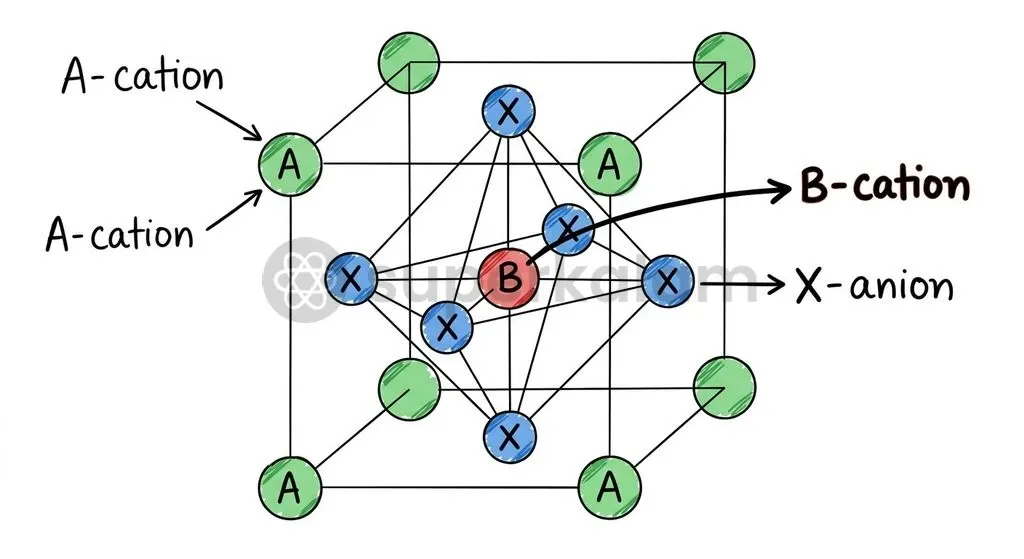
Perovskite photovoltaic absorbers share a distinct ABX3 crystal stoichiometry that facilitates rapid charge transport and broad spectral tunability. The material takes its name from Russian mineralogist L. A. Perovski, denoting compounds that mimic the crystal lattice structure of calcium titanate.
According to the Ossila Technical Guide, the $ABX_3$ architecture consists of three fundamental components:
- 'A' represents a monovalent cation: Common organic or inorganic examples include methylammonium, formamidinium, or caesium, which occupy the outer corner cavities of the crystal unit cell.
- 'B' represents a divalent metal cation: Centrally positioned metal ions such as lead or tin coordinate with surrounding halide anions.
- 'X' represents a halide anion: Halogen atoms including iodide, bromide, or chloride form corner-sharing octahedra around the central metal cation.
According to a review published by the Royal Society of Chemistry in Energy & Environmental Science, the optical bandgap of metal-halide perovskites is continuously tunable between approximately 1.2 electron-volts (eV) and 2.3 eV. Researchers adjust this bandgap by altering the halide anion ratio—such as the balance between iodine and bromine—or by tuning the cation composition. A wider bandgap lets the material absorb high-energy visible and ultraviolet photons while letting lower-energy light pass through unhindered.
Side-by-Side Breakdown: Perovskite vs Traditional Silicon Panels
Crystalline silicon and synthetic metal-halide perovskites represent fundamentally different manufacturing, structural, and thermodynamic paradigms. Silicon relies on established, capital-intensive metallurgy, whereas perovskites rely on agile, solution-based chemical synthesis.
| Evaluation Metric | Crystalline Silicon (c-Si) Panels | Metal-Halide Perovskite Cells | Perovskite-Silicon Tandem Configuration |
|---|---|---|---|
| Crystal Architecture | Diamond cubic covalent network | $ABX_3$ corner-sharing perovskite lattice | Stacked wide-bandgap top layer on bottom c-Si wafer |
| Material Bandgap | Fixed at 1.12 eV | Tunable between 1.2 eV and 2.3 eV | Split absorption: 1.7–1.8 eV (top) / 1.12 eV (bottom) |
| Thermodynamic Efficiency Limit | ~29.4% (Shockley-Queisser single-junction) | ~30.5% (single-junction equivalent limit) | Over 43% (detailed balance limit) |
| Thermal Processing Budget | High-temperature pulling exceeding 1414°C | Low-temperature synthesis below 150°C | Combined: standard wafering topped with low-temp printing |
| Manufacturing Footprint | Capital-intensive Czochralski ingot pulling and wafering | Solution-phase slot-die coating and roll-to-roll printing | Standard wafer lines with inline thin-film deposition add-ons |
| Warranted Operating Lifespan | Standard 25 to 30 years (<0.5% annual degradation) | Unproven commercial longevity; rapid moisture degradation | Emerging pilot warranties; subject to qualification benchmarks |
| Environmental Hazard Profile | Chemically stable; inert bulk material risks | Contains water-soluble divalent lead compounds | Contained lead hazard requiring hermetic encapsulation |
Silicon manufacturing demands heavy thermal energy. The International Energy Agency notes that conventional crystalline silicon production requires energy-intensive Czochralski crystal pulling from molten silicon at temperatures exceeding 1414°C. This requirement drives substantial embodied energy and necessitates large capital outlays for specialised cleanroom facilities.
In contrast, NREL documentation confirms that perovskite thin films can be deposited via low-temperature, solution-phase methods below 150°C. Techniques such as slot-die coating, blade coating, and roll-to-roll printing on flexible substrates lower the thermal budget and trim facility setup costs.
Discuss with Superkalam
Explain how spectral splitting works in a tandem architecture and why it reduces thermalisation losses compared to a single-junction cell.
Ask NowPartner Rather Than Rival? The Promise of Perovskite-Silicon Tandem Cells
Tandem solar configurations resolve the trade-off between silicon's proven durability and perovskite's superior absorption properties by stacking both materials into a complementary device. Research published in ACS Energy Letters demonstrates that multi-junction tandem architectures raise the theoretical maximum conversion efficiency to over 43% under un-concentrated standard solar illumination.
Nature reports that in a perovskite-silicon tandem cell, a wide-bandgap top perovskite layer (1.7–1.8 eV) captures high-energy blue and green photons. Lower-energy near-infrared light passes through to the narrow-bandgap bottom silicon cell (1.12 eV). This split-spectrum operation curtails thermalisation loss by generating electricity at higher operating voltages rather than dissipating surplus energy as heat.
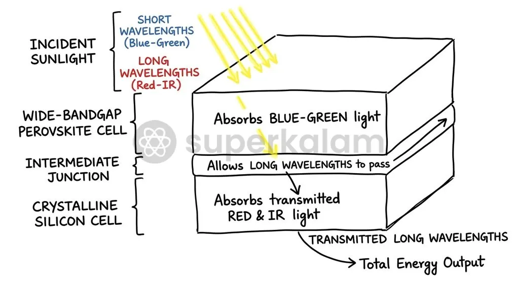
Laboratory and pilot certifications demonstrate that this tandem architecture proves viable outside theoretical modelling:
- Certified Laboratory Record: In July 2026, LONGi Green Energy achieved a certified power conversion efficiency of 35.5% for a two-terminal silicon-perovskite tandem laboratory cell, independently verified by the European Solar Test Installation.
- Commercial Format Demonstration: Fraunhofer CalLab certified a 26.9% module efficiency for Oxford PV on a 60-cell residential-format module, showing that efficiency gains translate to commercial sizes.
- Infrastructure Adaptability: As reported by PatSnap Insights in April 2026, perovskite-on-silicon tandems allow manufacturers to upgrade existing crystalline silicon lines by depositing a perovskite top layer rather than building new fabrication plants from scratch.
As an efficiency-boosting overlay, perovskites partner with existing silicon assets rather than mounting an immediate replacement.
The Durability Bottleneck: Moisture, Heat, and Commercial Viability Hurdles
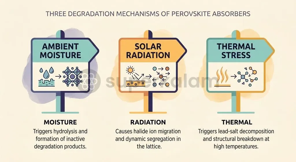
Commercial deployment of perovskite solar modules remains constrained by intrinsic material sensitivities to moisture, thermal variations, and environmental exposure. Silicon solar cells carry standard 25 to 30-year performance warranties with annual degradation rates below 0.5%. In contrast, perovskite cells struggle to maintain stable output outside controlled laboratory settings.
Primary degradation challenges hindering commercial readiness include:
- Moisture-Triggered Hydrolysis: According to the American Chemical Society, organic-inorganic hybrid perovskites are vulnerable to ambient moisture. Water ingress triggers rapid hydrolysis of organic cations like methylammonium, decomposing the photoactive crystal lattice into yellow lead iodide and volatile amine by-products:
$$\text{CH}_3\text{NH}_3\text{PbI}_3 \xrightarrow{\text{H}_2\text{O}} \text{PbI}_2 + \text{CH}_3\text{NH}_2 \uparrow + \text{HI}$$
(Degradation pathway showing phase collapse upon water contact)
- Photo-Induced Halide Segregation: Energy & Environmental Science highlights that wide-bandgap mixed-halide perovskites suffer from the Hoke effect under normal operational sunlight. Mixed iodide and bromide ions segregate into localised phase clusters, trapping charge carriers and causing significant open-circuit voltage losses across the cell.
- Toxicity and Environmental Leaching: Nature Sustainability reports that metal-halide perovskites contain water-soluble lead compounds that can leach divalent lead into groundwater systems if panels crack during extreme weather. Commercial viability therefore hinges on impermeable encapsulation barriers capable of passing rigorous stress standards.
Discuss with Superkalam
Compare the trade-offs between two-terminal (monolithic) and four-terminal tandem architectures regarding manufacturing integration and circuit complexity.
Ask NowPer TÜV Rheinland and Qcells, as reported in July 2026, commercial-scale perovskite-silicon tandem modules have successfully completed the full suite of IEC 61215 and UL 61215 qualification tests. This benchmark marks a critical milestone toward long-term operational durability.
Geopolitical Stakes: Can Perovskites Help India Bypass China's Silicon Dominance?
China's concentration of upstream silicon manufacturing creates strategic energy security risks for global solar installation targets. The International Energy Agency calculates that China controls more than 80% of global manufacturing capacity across all key stages of the crystalline silicon solar supply chain, exceeding 95% of global capacity for polysilicon ingots and wafers.
| Photovoltaic Manufacturing Stage | China Share | Rest of World Share |
|---|---|---|
| Polysilicon & Wafer Capacity | >95% | <5% |
| Cell & Module Assembly | >80% | <20% |
(Supply chain concentration across primary photovoltaic manufacturing steps)
This supply concentration leaves international solar markets exposed to single-source disruptions. In response, the Ministry of New and Renewable Energy is executing the Production Linked Incentive (PLI) Scheme for the National Programme on High Efficiency Solar PV Modules, backed by a ₹24,000 crore financial outlay across two tranches. In April 2023, the Solar Energy Corporation of India awarded contracts under Tranche-II to 11 manufacturers across three integration categories: fully integrated Polysilicon-to-Module, Wafer-to-Module, and Cell-to-Module.
Despite these investments, midstream dependencies persist. According to the Institute for Energy Economics and Financial Analysis, as of mid-2025, India's domestic manufacturing capacity stood at approximately 3.3 GW for polysilicon and 5.3 GW for wafers. This leaves domestic module assembly plants reliant on imported silicon wafers. Developing tandem-ready perovskite manufacturing offers a strategic avenue to leapfrog portions of the traditional supply chain, allowing domestic manufacturers to generate higher power output from existing wafer supplies.
Way Forward: R&D, Pilot Manufacturing, and India's Clean Energy Roadmap
Securing supply chain autonomy while hitting aggressive clean energy targets requires India to pursue a dual-track strategy spanning domestic industrial incentives and targeted laboratory research. Rather than attempting to replicate legacy, energy-intensive silicon supply chains from scratch, public and private stakeholders can direct capital toward hybrid tandem manufacturing architectures.
Key strategic levers for this transition include:
- Incentivising Tandem Technology under Future PLI Rounds: The Ministry of New and Renewable Energy can incorporate dedicated efficiency brackets into future solar incentive programmes, awarding capital support to firms building perovskite-compatible deposition lines on top of standard silicon cells.
- Targeted Materials Research via CSIR Labs: The Council of Scientific and Industrial Research can prioritise indigenous materials science programmes aimed at developing lead-free non-toxic metal cations, such as tin-based alternatives, and moisture-resistant barrier coatings.
- Standardising Accelerated Environmental Testing: India's testing institutions must implement specialised environmental stress testing that assesses tandem cells against high ambient humidity and elevated tropical temperatures, mirroring IEC standards.
- Leveraging International Solar Alliance Partnerships: India can use the International Solar Alliance framework to establish shared testing facilities and joint intellectual property consortiums with global institutions, lowering the capital expenditure required for pilot commercial production.
Discuss with Superkalam
Propose policy modifications for future rounds of India's Solar PLI Scheme to accelerate the transition from pure silicon wafers to tandem-ready cells.
Ask NowKey Takeaways
- Single-junction crystalline silicon modules face a thermodynamic ceiling defined by the Shockley-Queisser limit of 29.4%, driven by Auger recombination and thermalisation energy losses.
- Synthetic perovskites feature an $ABX_3$ crystal architecture with a tunable optical bandgap between 1.2 eV and 2.3 eV, allowing targeted absorption of high-energy blue-spectrum sunlight.
- Perovskite-silicon tandem cells overcome single-material limitations by combining a wide-bandgap top perovskite layer with a narrow-bandgap bottom silicon cell, raising theoretical maximum efficiencies above 43%.
- Operational durability remains the primary commercial bottleneck, with perovskites vulnerable to moisture-induced lattice breakdown, photo-induced halide segregation (Hoke effect), and lead-leaching risks.
- With China controlling more than 95% of global polysilicon and wafering capacity, developing perovskite-silicon tandem integration offers India a technological bridge to boost solar power output while managing upstream supply risks.
Mains Question
"Tandem integration offers a pathway beyond rigid thermodynamic limits without scrapping existing manufacturing lines." Elucidate the technological principles behind perovskite-silicon tandem cells and evaluate their potential to enhance India's domestic solar manufacturing. (15 Marks)
Evaluate NowMains Question
While perovskite photovoltaics promise breakthrough conversion efficiencies, operational durability and upstream supply concentration remain formidable bottlenecks. Critically examine. (10 Marks)
Evaluate NowPractice MCQs
QUESTION 1
With reference to solar photovoltaic technologies, consider the following statements:
- Single-junction crystalline silicon cells are constrained by the Shockley-Queisser thermodynamic efficiency limit of approximately 29.4%.
- Crystalline silicon has an adjustable optical bandgap, whereas metal-halide perovskites feature a fixed bandgap of 1.12 eV.
- Tandem solar cell configurations combining perovskite and silicon absorbers have a theoretical detailed balance efficiency limit exceeding 40%. Which of the statements given above are correct?
QUESTION 2
Consider the following statements regarding the structural and operational properties of perovskite solar cells:
- Perovskite absorbers adopt an ABX3 crystal lattice stoichiometry mimicking calcium titanate.
- In tandem architectures, the perovskite layer is placed at the bottom to absorb lower-energy infrared photons.
- Photo-induced phase segregation in mixed-halide perovskites under sustained illumination is termed the Hoke effect. Which of the statements given above is/are correct?
QUESTION 3
Regarding the commercialisation and manufacturing of perovskite solar cells, consider the following statements:
- Unlike traditional silicon ingots that require thermal processing exceeding 1400°C, perovskites can be synthesised via low-temperature solution processes below 150°C.
- Perovskite modules currently match crystalline silicon panels with commercial warranties exceeding 25 to 30 years.
- In four-terminal tandem designs, the top and bottom sub-cells are electrically connected in series, requiring strict current matching. Which of the statements given above is/are correct?
QUESTION 4
Which of the following phenomena is a primary thermodynamic cause limiting the conversion efficiency of single-junction crystalline silicon cells below the Shockley-Queisser ceiling?
QUESTION 5
With reference to India's solar photovoltaic manufacturing landscape, consider the following statements:
- The Production Linked Incentive (PLI) Scheme for High Efficiency Solar PV Modules is administered by the Ministry of New and Renewable Energy.
- China accounts for over 95% of global polysilicon and wafer manufacturing capacities.
- As of mid-2025, India's domestic wafer manufacturing capacity exceeded its domestic polysilicon capacity. Which of the statements given above is/are correct?