GS 3: EconomyGS 3: Science & TechnologyGS 2: GovernancePrelims
Modi inaugurates semiconductor facility in Gujarat, Pg1
PM Modi inaugurates CG Semi's semiconductor assembly facility in Sanand, Gujarat, boosting India's tech manufacturing and creating large-scale employment.
Practice MCQs
804 Students attempted
Key Highlights:
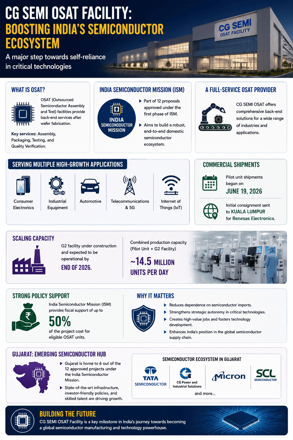
- Prime Minister Narendra Modi inaugurated the CG Semi Outsourced Semiconductor Assembly and Test (OSAT) facility in Sanand, Gujarat, on July 4, 2026.
- The facility is a joint venture involving CG Power and Industrial Solutions Limited, Renesas Electronics Corporation, and Stars Microelectronics.
- This project represents an investment of over ₹7,600 crore and has commenced commercial production.
- The plant is designed to initially produce 200 million chips annually, with a long-term target of 500 crore chips per year.
- The inauguration marks a significant milestone in India's efforts to establish itself as a global semiconductor manufacturing hub.
SEMI-OSAT.png
Detailed Insights:
- The CG Semi facility in Sanand is one of India's first full-scale OSAT plants, with a second facility (G2) currently under development.
- This initiative is a crucial component of the India Semiconductor Mission (ISM), which aims to foster a robust domestic semiconductor and display ecosystem.
- The facility will produce both traditional and advanced semiconductor packages, catering to critical sectors such as automotive, Internet of Things (IoT), industrial, and 5G technologies.
- The project is expected to generate substantial employment opportunities and reduce India's dependence on imported semiconductor chips.
- Government support for such manufacturing units is provided through schemes like the Production Linked Incentive (PLI) Scheme for semiconductors, launched in 2021.
- The OSAT plant performs essential post-fabrication processes, including the assembly, packaging, testing, and inspection of semiconductor devices.
Scientific/Technical Concepts Involved:
- Semiconductor: A material with electrical conductivity between a conductor and an insulator, fundamental to modern electronic devices.
- Outsourced Semiconductor Assembly and Test (OSAT): Third-party companies that provide specialized services for the assembly, packaging, and testing of semiconductor chips after they have been fabricated.
- Wafer Fabrication: The process of manufacturing integrated circuits on semiconductor wafers, typically silicon, before they are cut into individual dies.
- Semiconductor Packaging: The process of enclosing a semiconductor die in a protective casing to prevent damage and corrosion, while also providing electrical connections for integration into electronic systems.

SuperKalam is your personal mentor for UPSC preparation, guiding you at every step of the exam journey.
Download the App


STUDY RESOURCES
CONTACT US
ⓒ Snapstack Technologies Private Limited