GS 2: GovernanceGS 3: Science & TechnologyGS 2: International RelationsGS 3: EconomyPrelims
A semiconductor vision beyond the shop floor, Pg12
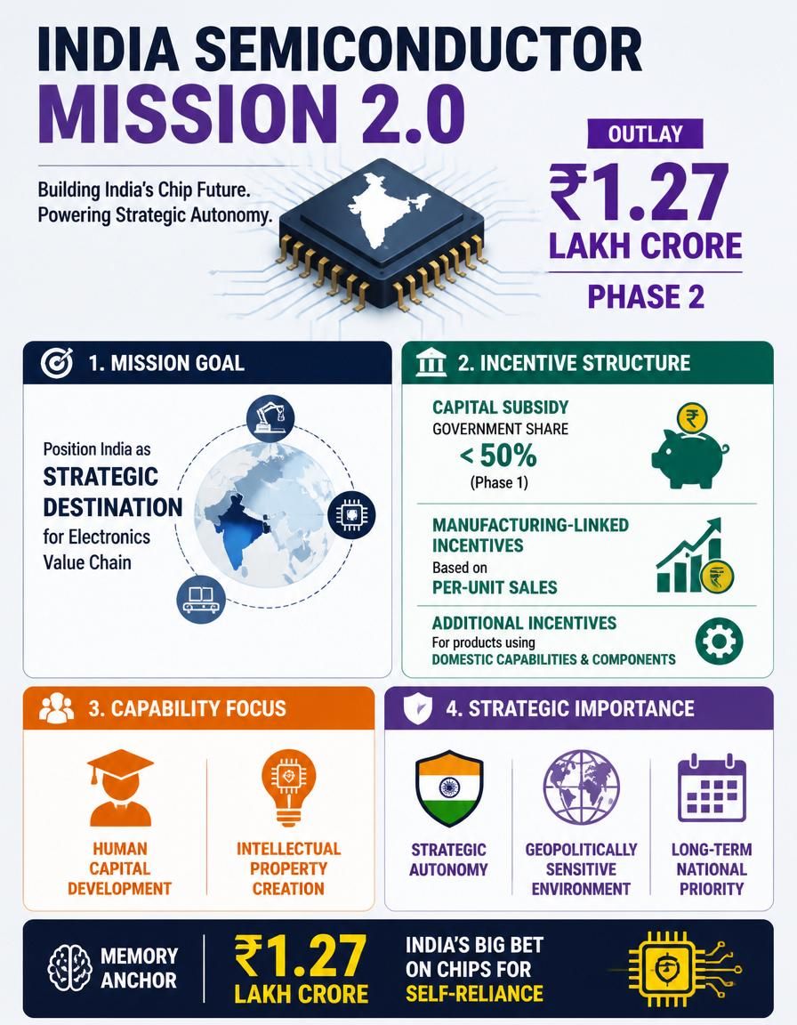
Union Cabinet approves Rs 1.27 lakh crore India Semiconductor Mission Phase 2, pivoting to chip design and innovation for global tech leadership.
Practice MCQs
898 Students attempted
Key Highlights:
- The Union Cabinet approved the second phase of the India Semiconductor Mission, shifting focus from manufacturing to building an innovation landscape.
- An outlay of Rs 1,27,500 crore has been announced to primarily facilitate semiconductor design, a high-value segment of the industry.
- The policy redirects fiscal support from fabrication units towards companies producing raw materials, speciality chemicals, and industrial gases.
- Subsidies of up to 75 per cent are offered for chip design, underscoring the emphasis on Research and Development (R&D).
- India aims to establish an ecosystem for manufacturing mature node chips (28 nm or larger), which constitute approximately 70% of global semiconductor demand.
- An aspirational goal is set to develop 7nm and 2nm chips within the next five years.
ISM 2.0.jpg
Detailed Insights:
- The second phase of the India Semiconductor Mission seeks to integrate chip design, equipment, materials, intellectual property, and advanced research into a cohesive industrial strategy.
- Countries can secure pivotal positions in global supply chains through expertise in chip architecture, verification, software, and intellectual property, even without advanced fabrication plants.
- The policy aligns with India's comparative advantages by focusing on mature node chips, which are essential for a wide range of applications including electronics, smartphones, power grids, and medical devices.
- The global semiconductor market has experienced significant disruptions due to factors like the Covid pandemic and ongoing tech rivalries, highlighting the strategic importance of the sector.
- Major global powers such as the US, China, South Korea, Taiwan, the Netherlands, and Japan leverage their semiconductor capabilities as strategic assets.
- Developing robust semiconductor capabilities necessitates reliable power infrastructure, precise logistics, predictable environmental clearances, and a substantial pool of skilled technicians.
- India aims to convert its existing strength in semiconductor design, evidenced by global firms' design centers in cities like Bengaluru, Hyderabad, Pune, and Noida, into world-class manufacturing capacity.
- The government's role is crucial as an enabler, fostering strong linkages between academia and industry, drawing parallels with successful models in Taiwan, South Korea, and the US.
Key Concepts Involved:
- India Semiconductor Mission: A government initiative aimed at fostering a robust semiconductor and display manufacturing ecosystem within India.
- Mature Node Chips: Semiconductor chips produced using established, larger process technologies, typically 28 nanometers (nm) or greater.
- Chip Design: The process of conceptualizing and creating the functional and physical specifications for integrated circuits or microchips.
- Intellectual Property (IP): Legal rights granted to creators for their original works, inventions, or designs, crucial for innovation in the semiconductor industry.

SuperKalam is your personal mentor for UPSC preparation, guiding you at every step of the exam journey.
Download the App


STUDY RESOURCES
CONTACT US
ⓒ Snapstack Technologies Private Limited