GS 2: GovernanceGS 3: Science & TechnologyGS 3: EconomyPrelimsGS 3: Changes in Industrial Policy and Effects on Industrial Growth
To cash in on next tech boom, India needs the right chips, Pg11
India must pivot its semiconductor strategy from low-margin assembly to high-margin design and advanced fabrication for future AI economy leadership.
Practice MCQs
804 Students attempted
Key Highlights:
- India aims to become a principal player in the global semiconductor and AI economy, recognizing technology as the foundation for economic growth.
- Current initiatives like the India Semiconductor Mission (ISM), Design Linked Incentive (DLI), and IndiaAI Mission are foundational steps.
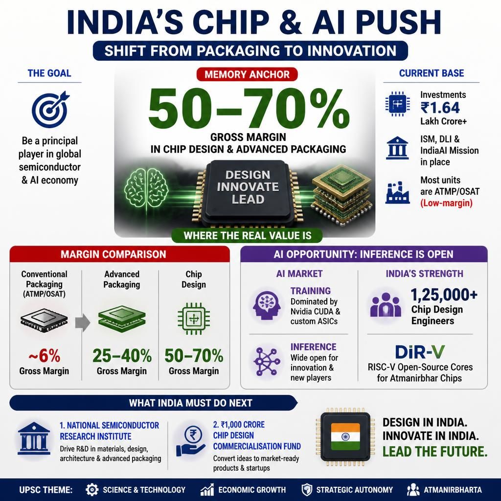
- Despite significant investment commitments of over ₹1.64 lakh crore, a structural problem exists with most approved units being low-margin ATMP/OSAT facilities.
- The focus needs to shift from basic packaging to high-margin chip design and advanced packaging, which offer 50-70% gross margins.
- Key recommendations include establishing a National Semiconductor Research Institute and a ₹1,000-crore Chip Design Commercialisation Fund.
- India possesses a large talent pool of 1,25,000 chip design engineers and programs like DIR-V for RISC-V open-source cores, positioning it well for AI inference chip development.
India's Chip.jpg
Detailed Insights:
- Nations like Taiwan, South Korea, and China have made substantial investments in semiconductor mastery and self-sufficiency, with the US passing the CHIPS Act for significant subsidies.
- India's strengths lie in its demographic scale and intellectual capital, with engineers and scientists at the forefront of global AI and semiconductor development.
- Historically, India has underinvested in technological sovereignty, risking exclusion from critical technologies due to geopolitical moves like restrictions on AI models.
- The success of the electronics Production Linked Incentive (PLI) scheme, which led to India assembling 25-28% of global iPhones, was based on supply-chain diversification.
- Semiconductors are undergoing an architectural revolution driven by AI, creating new value in compute, unlike the supply-chain diversification seen in electronics.
- While conventional wire-bond packaging yields around 6% gross margins, advanced packaging and chip design offer significantly higher margins of 25-70%.
- The AI market is bifurcated into training (dominated by Nvidia's CUDA ecosystem and custom ASICs) and inference, with the latter being wide open for innovation.
- India's IndiaAI's sovereign EIGN compute programme, defence procurement, 5G infrastructure, and a billion-user domestic market provide ready demand for inference chips.
- The National Investment and Infrastructure Fund (NIIF) model is suggested for the proposed Chip Design Commercialisation Fund to support fabless companies.
Key Concepts Involved:
- India Semiconductor Mission (ISM): A government initiative to build a robust semiconductor and display ecosystem in India, positioning it as a global manufacturing and design hub.
- Design Linked Incentive (DLI): A scheme offering financial incentives and design infrastructure support to companies engaged in semiconductor design and innovation.
- ATMP/OSAT: Assembly, Testing, Marking, and Packaging (ATMP) refers to the manufacturing process, while Outsourced Semiconductor Assembly and Test (OSAT) refers to third-party companies providing these services.
- RISC-V: An open-source instruction set architecture (ISA) that allows for the development of custom processors without licensing fees, promoting innovation.
- ASICs: Application-Specific Integrated Circuits are custom-designed chips optimized for a particular application or function, offering high performance and efficiency for specific tasks.
- CUDA: Nvidia's proprietary parallel computing platform and API that enables software to use GPUs for accelerated general-purpose processing, crucial for AI and scientific computing.

SuperKalam is your personal mentor for UPSC preparation, guiding you at every step of the exam journey.
Download the App


STUDY RESOURCES
CONTACT US
ⓒ Snapstack Technologies Private Limited