GS 2: GovernanceGS 3: Science & TechnologyGS 3: EconomyPrelimsGS 3: Changes in Industrial Policy and Effects on Industrial Growth
Semicon 2.0: How India Aims To Build A Domestic Chip Design Ecosystem, Pg15
India launches Rs 1.27 lakh crore Semicon 2.0 program to build a domestic chip design ecosystem, offering incentives for strategic technologies.
Practice MCQs
797 Students attempted
Key Highlights:
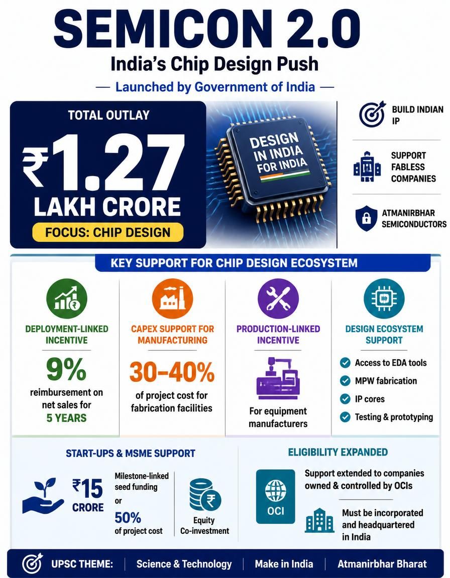
- The Centre has launched Semicon 2.0, a Rs 1.27 lakh crore program, to foster a domestic chip design ecosystem in India.
- The program's primary focus is on chip design, with dedicated tracks for strategic semiconductor technologies and commercially viable products.
- It aims to boost Indian-owned intellectual property and support fabless semiconductor companies by providing access to tools and funding.
- A deployment-linked incentive offers 9% reimbursement on net sales for five years to help newly designed chips find market adoption.
- The scheme also provides capital expenditure support (30-40%) for manufacturing facilities and a Production-Linked Incentive for equipment manufacturers.
SEMICON 2.0.jpg
Detailed Insights:
- Semicon 2.0 addresses a critical gap where India has a strong chip-design engineering talent pool but lacks significant Indian-owned intellectual property.
- The program's first pillar is entirely dedicated to design, covering chips for national security and critical infrastructure, as well as commercial applications.
- For commercial chip design, the government offers access to expensive Electronic Design Automation (EDA) tools, Multi-Project Wafer (MPW) fabrication services, and IP cores.
- Start-ups and MSMEs can receive milestone-linked seed funding up to Rs 15 crore or 50% of the project cost, along with potential equity co-investments.
- Eligibility for commercial design support has been extended to companies owned and controlled by Overseas Citizens of India (OCIs), provided they are incorporated and headquartered in India.
- The deployment-linked incentive is crucial for young fabless companies to overcome challenges in convincing manufacturers to adopt new Indian chips over established overseas suppliers.
- Beyond design, the scheme supports the broader semiconductor supply chain, including R&D facilities, manufacturing of wafers, photomasks, chemicals, and testing facilities.
- Large silicon wafer fabs are eligible for higher capital expenditure support of 40%.
Key Concepts Involved:
- Fabless Semiconductor Companies: Firms that design and sell integrated circuits but outsource their physical manufacturing to third-party foundries.
- Electronic Design Automation (EDA) Tools: Software tools used for designing, verifying, and manufacturing electronic systems, including integrated circuits.
- Multi-Project Wafer (MPW) Fabrication: A cost-effective method allowing multiple chip designs from different companies to be fabricated on a single silicon wafer.
- IP Cores: Reusable blocks of logic or data that can be integrated into a larger chip design, saving development time and cost.
- System-on-Chip (SoC): An integrated circuit that integrates all components of a computer or other electronic system into a single chip.
- Production-Linked Incentive (PLI) Scheme: A government initiative to boost domestic manufacturing and exports by offering incentives on incremental sales.

SuperKalam is your personal mentor for UPSC preparation, guiding you at every step of the exam journey.
Download the App


STUDY RESOURCES
CONTACT US
ⓒ Snapstack Technologies Private Limited