GS 2: GovernanceGS 3: Science & TechnologyGS 3: EconomyPrelimsGS 3: Changes in Industrial Policy and Effects on Industrial Growth
Amount Outlined for Semicon Programme by Government, Pg8
Government notifies ₹1.27 lakh crore Semicon 2.0 program, offering 40% fiscal support for silicon wafer fabs and chip design incentives.
Practice MCQs
790 Students attempted
Key Highlights:
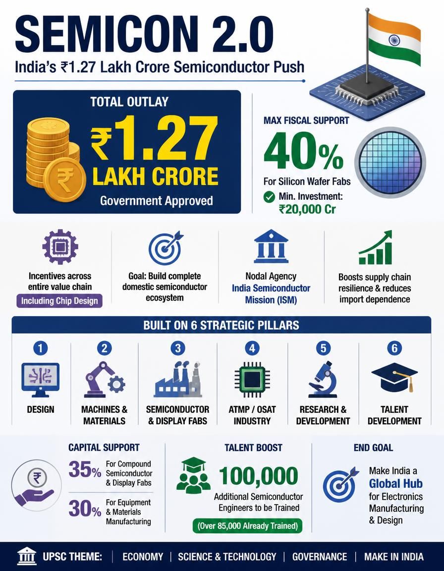
- The government has officially notified the Semicon 2.0 programme with a total outlay of ₹1.27 lakh crore.
- The programme offers 40% fiscal support for silicon wafer fabrication units requiring a minimum investment of ₹20,000 crore.
- Incentives are also extended across the entire semiconductor value chain, including chip design.
- Semicon 2.0 aims to foster a comprehensive domestic semiconductor ecosystem in India.
- The India Semiconductor Mission (ISM) operates as the nodal agency responsible for the programme's implementation.
Semicon 2.0.jpg
Detailed Insights:
- Semicon 2.0 builds upon the initial Semicon India Programme (Semicon 1.0), which was approved in December 2021 with a financial outlay of ₹76,000 crore.
- The expanded programme is structured around six key pillars: design, machines and materials, semiconductor and display fabs, ATMP/OSAT industry, research and development, and talent development.
- It provides 35% capital expenditure support for compound semiconductor fabs and display fabs, and 30% for semiconductor equipment and materials manufacturing.
- The initiative seeks to enhance India's supply chain resilience, reduce import dependence, and establish the country as a global hub for electronics manufacturing and design.
- India aims to train an additional 100,000 semiconductor engineers under this programme, building on the 85,000 already developed.
- The programme includes provisions for seed funding and access to design infrastructure for startups and MSMEs involved in chip design.
- India's domestic semiconductor market is projected to grow significantly, reaching an estimated $110-120 billion by 2030.
Key Concepts Involved:
- Semiconductor Manufacturing: The complex process of fabricating integrated circuits (chips) that are essential components of all electronic devices.
- Silicon Wafer Fabs: Highly advanced manufacturing facilities where silicon wafers are processed through numerous steps to create semiconductor devices.
- Chip Design: The engineering process of creating the logical and physical layout of an integrated circuit before it is manufactured.
- Fiscal Support: Financial assistance provided by the government to industries or projects, typically through subsidies, grants, or tax incentives, to encourage growth and investment.

SuperKalam is your personal mentor for UPSC preparation, guiding you at every step of the exam journey.
Download the App


STUDY RESOURCES
CONTACT US
ⓒ Snapstack Technologies Private Limited